Front-End Semiconductor Fabrication
CMP Slurry
CMP Slurry (Polishing Slurry)
In advanced semiconductor manufacturing, Chemical Mechanical Polishing (CMP) is a critical step for wafer planarization.
Scientia leverages high-quality CMP slurry products from leading supplier to provide a comprehensive portfolio covering oxide, tungsten, polysilicon and ceria-based slurries. These products help customers balance removal rate, selectivity and defect control across different process steps and achieve a stable, high-yield process window.
Sputtering Targets
High Purity × Diverse Materials × Precision Manufacturing
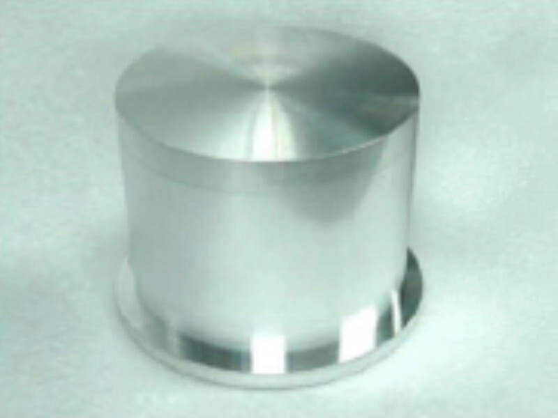
Scientia supplies high-purity sputtering targets that are widely used in the semiconductor, optoelectronics, and precision electronics industries. In advanced processes and thin-film deposition, the purity and stability of the target material play a decisive role in film performance and production yield. With strict process control, we deliver sputtering targets up to 5N (99.999%) purity, meeting the demanding requirements for material consistency and reliability in high-end semiconductor manufacturing.
Precious Metal Target Recycling
Cost Reduction × High Purity Refining × Supply Chain Stability
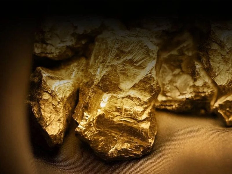
Scientia provides precious metal sputtering target recycling services, transforming used targets into high-purity metals through advanced refining and re-manufacturing process. This service enables customers to reduce sputtering target costs while enhancing supply chain security and efficiency.
Dummy Wafer
Stable Performance × Cost Control
Scientia Corporation supplies high-quality dummy wafers designed to reduce consumable costs in semiconductor process testing, equipment calibration, and tool maintenance, while maintaining stable process accuracy and reliability.
Reclaim Wafer
Cost Efficiency × Near-Pristine Quality
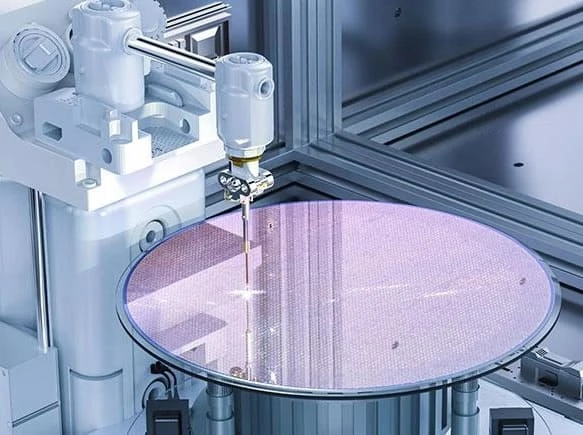
Scientia provides professional reclaim wafer services, specializing in 6-inch, 8-inch, and 12-inch wafer recycling and re-manufacturing.
By leveraging advanced grinding, polishing, and inspection techniques, our reclaim wafers match the quality of new wafers in flatness, particle control, and metal purity—empowering customers to cut costs while ensuring high process reliability.
PVD Components
Film Stability × Yield Improvement
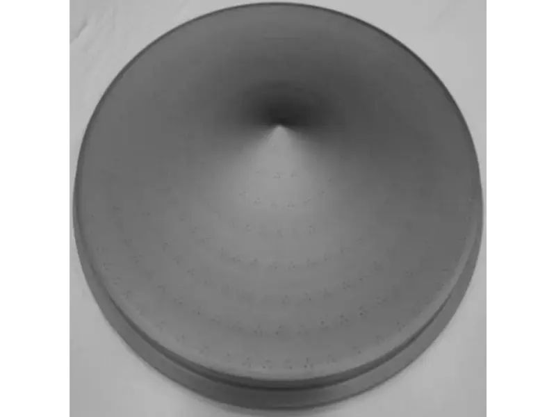
PVD (Physical Vapor Deposition) is a core thin-film technique in semiconductor and precision manufacturing. By physically evaporating or sputtering materials to form uniform coatings on wafers or workpieces, PVD improves surface conductivity, wear resistance, and protection.
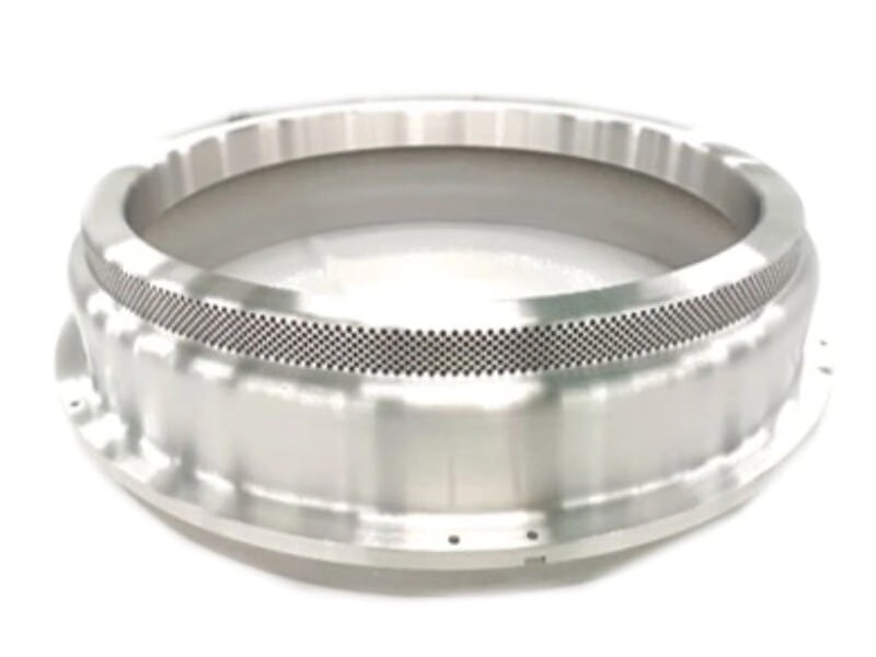
Scientia supplies compatible PVD process components (process consumables & parts) to stabilize deposition quality and enhance yield.
CVD Components
Precision Control × High-Uniformity Deposition
CVD (Chemical Vapor Deposition) is a critical thin-film technique in semiconductor manufacturing, utilizing high temperatures to distribute reactive gases evenly across wafer surfaces. Through controlled chemical reactions, films are formed with excellent uniformity, stability, and reproducibility. Widely applied to insulating layers, protective coatings, diffusion layers, and epitaxial wafers, CVD plays a vital role in advanced device fabrication.
Scientia provides a full range of CVD process components (CVD parts) to ensure film quality and process stability.
Etch Process Components
Non-Metal Parts|Corrosion Resistance × Precision Engineering
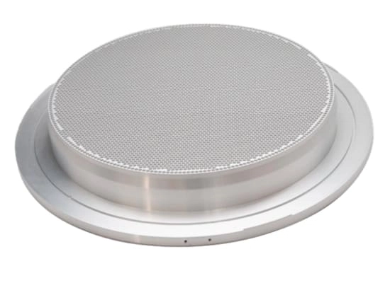
In semiconductor etching, non-metal components play a critical role in withstanding plasma environments, high temperatures, and corrosive gases, while maintaining process stability and accuracy.
Scientia provides a wide range of quartz (QTZ) and silicon (Si) parts, precisely manufactured to meet the stringent requirements of advanced etch processes.
Specialty Gases
High Purity Supply × Diverse Process Applications
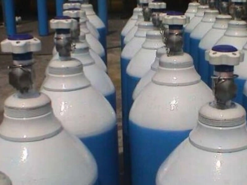
Scientia distributes high-purity specialty gases engineered for semiconductor, optoelectronics, and precision manufacturing processes. Our portfolio covers electronic gases, mixed gases, metal-organic compounds (MOCVD precursors), and fine chemicals, supporting diverse applications including front-end processing, thin-film deposition, etching, and packaging.
Working with original manufacturers that provide production, purification, and distribution capabilities, we ensure consistent quality, reliable supply, and stable performance across advanced manufacturing lines.

