Model number: p-04
Reclaim Wafer
Cost Efficiency × Near-Pristine Quality
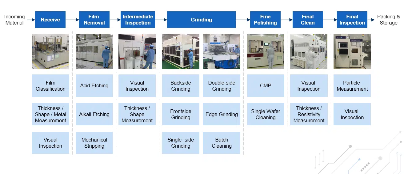
Scientia provides professional reclaim wafer services, specializing in 6-inch, 8-inch, and 12-inch wafer recycling and re-manufacturing.
By leveraging advanced grinding, polishing, and inspection techniques, our reclaim wafers match the quality of new wafers in flatness, particle control, and metal purity—empowering customers to cut costs while ensuring high process reliability.
Key Features & Advantages
Full-Size Coverage
- Available in 6-inch, 8-inch, and 12-inch sizes.
- Comparable to new wafers with low particles, low metal contamination, and low haze—reducing costs while maintaining precision.
Excellent particle control
- ≥26 nm particles: ≤200 ea
- 12-inch wafer (typical): only 27 ea
High Flatness
- GBIR average: 1.62 μm (≤10 μm)
Ultra-Low Metal Contamination
- ≤1E9 atoms/cm²
Low Haze
- Average: 0.051 ppm (≤0.2 ppm)
Stable Lead Times
- Supported by in-house production and strict scheduling for consistent delivery.
Comparison
New Dummy Wafers vs. Reclaim Dummy Wafers (Scientia)
| Category | New Dummy Wafer | Reclaim Dummy Wafer(Scientia) |
|---|---|---|
| Material Cost |
High (depending on wafer size and supplier) | Low (cost savings over 50%) |
| Process Precision |
High (excellent surface quality and thickness uniformity) | High (precision polishing and inspection, comparable to new wafer standards) |
| Environmental Impact | Low (high energy consumption and carbon emissions in production) | High (recycled and re-manufactured, reduces wafer waste and carbon footprint) |
| Lead Time | Long (dependent on global silicon wafer supply chain) | Short (in-house production with flexible scheduling, supports mass delivery) |
12-inch Reclaim Wafers
| Item | Target | Process Capability | ||
|---|---|---|---|---|
| AVG | Sigma | |||
| Particle | 26nm | ≤ 200ea | 27ea | 19 |
| 37nm | ≤ 100ea | 20ea | 15 | |
| 45nm | ≤ 80ea | 15ea | 11 | |
| 65nm | ≤ 60ea | 9ea | 8 | |
| 90nm | ≤ 40ea | 6ea | 5 | |
| 120nm | ≤ 30ea | 4ea | 4 | |
| GBIR(TTV) | 10μm | 1.62μm | 0.61 | |
| Haze | 0.2ppm | 0.051 | 0.015 | |
| Cu, Na, Al, Ca, K, Cr, Fe, Ni, Zn, Li, Mg, W, Mo, Co, K, Mn,TI (SURFACE) |
≤ 1E10 atoms/cm² | 1E9 atoms/cm² | ||
6-inch & 8-inch Reclaim Wafers
| Item | Specification | Remark | |||||
|---|---|---|---|---|---|---|---|
| 8 inch general test | 6 inch general test | 6 inch prime or specified | |||||
| 1. GENERAL CHARACTERISTICS | |||||||
| 1.1 | 生長方式 | Growth Method | cz | cz | cz | ||
| 1.2 | 晶向 | Crystal Orientation | <100> + 1.0 degrees | <100> + 1.0 degrees | <100> + 1.0 degrees | ||
| 1.3 | 導電型 | Conductivity Type | P or N -Type | P or N -Type | P or N -Type | ||
| 1.4 | 摻雜劑 | Dopant | B/Ph | B/Ph | B/P/Sb/As | ||
| 1.5 | 邊緣不計 | Nominal Edge Exclusion | 3 or 5 mm | 3 or 5 mm | 3 or 5 mm | ||
| 2. ELECTRICAL CHARACTERISTICS | |||||||
| 2.1 | 電阻率 | Resistivity | 0.1-1000hm-cm | 0.1-1000hm-cm | 0.001-1000hm-cm | ||
| 3. MECHANICAL CHARACTERISTICS | |||||||
| 3.1 | 直徑 | Diameter | 200 + 0.5 mm | 150 + 0.5 mm | 50 + 0.5 mm | ||
| 3.2 | V型槽深度 | Notch Depth | NOTCH | NOTCH or FLAT | NOTCH or FLAT | ||
| 3.3 | V型槽晶向 | Notch Orientation | <110> + 1. O degrees | <110> + 1. O degrees | <110> + 1. O degrees | ||
| 3.4 | 倒角輪廓 | Edge Shape | SEMI S1 | SEMI S1 | SEMI | ||
| 3.5 | 厚度 | Thickness | >550um | >500um | >500um | ||
| 3.6 | 彎曲度 | Bow | <=60um | <=60um | <=50um | ||
| 3.7 | 翹曲度 | Warp | <=60um | <=60um | <=50um | ||
| 3.8 | 總厚度變化 | TTV | <=25um | <=25um | <=10um | ||
| 3.9 | 全貌平整度 | TIR | NA | NA | <=5um | ||
| 4. FRONT SURFACE CHEMISTRY | |||||||
| 4.1 | 表面金屬 | Surface Metal Contamination | |||||
| Na, AI,Ca,K,Fe,Cr,Cr, Cr, Ni, Zn | <=5xE10 /cm2 | <=5xE10 /cm2 | <=5xE10 /cm2 | ||||
| 5. FRONT SURFACE CRITERIA | |||||||
| 5.1 | 刮傷 | Scratches | None | None | None | ||
| 5.2 | 顆粒要求 | LPD particle | >=0.2um | <=30 | <=30 | <=30 | |
| 6. BACK SURFACE CRITERIA | |||||||
| 6.1 | 亮點 | Brightness (Gloss) | Free | Free | Free | ||
| 6.2 | 划傷總長度 | Scratches (micro) (total length) | < Diameter | < Diameter | |||
| 6.3 | 沾污 | Stain | Free | Free | Free | ||
| 6.4 | 崩邊 | Chips | Free | Free | Free | ||

