


Model number: p-07
CVD Components
Precision Control × High-Uniformity Deposition
CVD (Chemical Vapor Deposition) is a critical thin-film technique in semiconductor manufacturing, utilizing high temperatures to distribute reactive gases evenly across wafer surfaces. Through controlled chemical reactions, films are formed with excellent uniformity, stability, and reproducibility. Widely applied to insulating layers, protective coatings, diffusion layers, and epitaxial wafers, CVD plays a vital role in advanced device fabrication.
Scientia provides a full range of CVD process components (CVD parts) to ensure film quality and process stability.
Expert in Semiconductor Showerheads and Faceplates
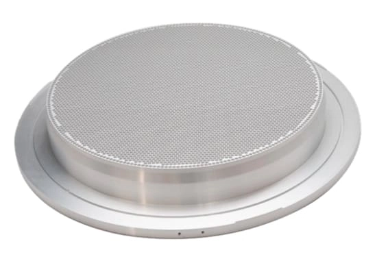
In the highly precise world of semiconductor manufacturing, every consumable inside the chamber plays a critical role in overall yield. We focus on providing high-purity, high-precision replacement parts for Lam Research gas distributors (Showerheads) and Applied Materials (AMAT) gas distribution plates (Faceplates).
Our products are designed to match OEM standards in quality, while leveraging an optimized supply chain and professional engineering support to keep your production line running at maximum efficiency and minimum operating cost.
Choosing us means choosing a high-performance, cost-effective and seamlessly compatible solution.
Service Advantages
We understand the stringent requirements of the semiconductor industry for quality, lead time and technical expertise. Our service commitment is to be the most reliable technical backbone behind your production line.
Customized Solutions
For specific processes or non-standard tool requirements, we offer flexible customized design and manufacturing services. Whether it is material control, hole-density optimization, special hole machining or customized surface treatments, we can help you enhance the performance of your targeted processes.
Cost Competitiveness
With an optimized global supply chain and highly efficient manufacturing, we provide cost-effective key consumables. We help significantly reduce your operating costs without compromising on quality.
Experienced Engineering Team
Our team is composed of engineers with decades of semiconductor process experience. We are not only a parts supplier but also a technical consultant who can engage in in-depth discussions with your process and procurement teams, and help you resolve yield and lifetime challenges on the production floor.
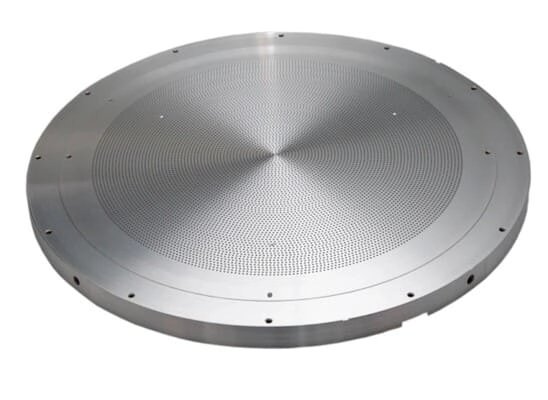
Lam Research Showerhead
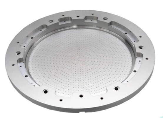
The showerhead is one of the most critical gas distribution components in plasma etch or deposition chambers. Its performance directly determines process uniformity and yield.
Key Features:
-
Uniform precursor gas distribution
The internal channels and micro-hole design of the showerhead are optimized specifically for CVD gas flow. They ensure that all reactive gases are delivered to the wafer surface with precise angles and flow rates, forming the foundation for highly uniform film thickness. -
PECVD plasma control
In PECVD applications, the showerhead also functions as an RF electrode. Its material and structure directly affect the electric field distribution of the plasma and precisely control ion energy, which in turn determines film density, stress and dielectric constant (k-value). -
Accurate thermal management
The showerhead must maintain accurate temperature control to prevent precursor gases from prematurely decomposing or condensing before entering the chamber. Proper thermal design helps reduce particle defects and maintain a clean process environment. -
Corrosion and build-up resistance
Made from high-purity, corrosion-resistant materials, the showerhead minimizes the build-up of reaction by-products (such as oxide or nitride residues) on its surface. This extends cleaning intervals and contributes to long-term process stability.
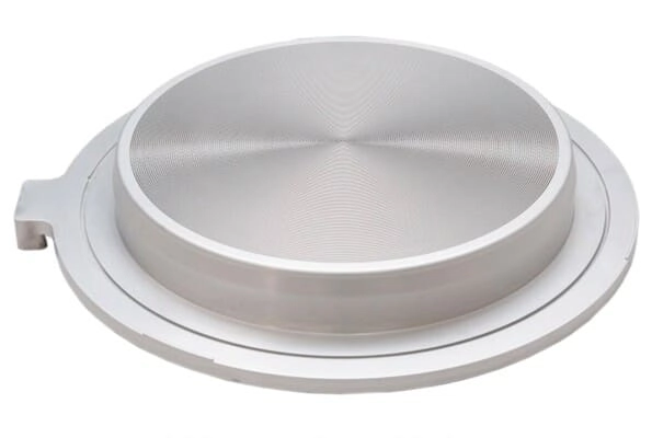
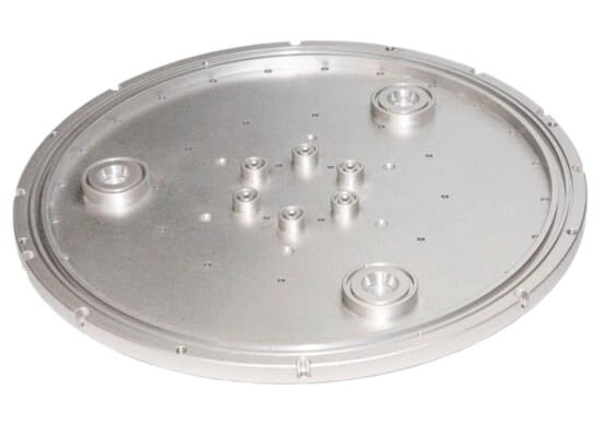
AMAT Faceplate
In AMAT CVD tools, such as PECVD systems, the faceplate is located at the top of the reaction zone and plays a key role in gas flow control and heat transfer. It is indispensable for depositing high-performance films efficiently.
Key Features:
-
Laminar flow of reactive gases
The unique geometry of the faceplate is designed to guide gases coming from the showerhead into a stable laminar flow. This maximizes the delivery of precursors to the wafer surface and is critical for step coverage in high aspect-ratio structures. -
Thermal uniformity and film stress
As a key element in the thermal path inside the chamber, the faceplate’s thermal stability and thermal conductivity affect the temperature uniformity above the wafer. This controls the intrinsic stress of the film and helps prevent peeling or cracking. -
Contamination and by-product isolation
During deposition, the faceplate effectively isolates or captures reaction by-products in non-target areas, reducing the risk of particles falling onto the wafer surface. This is crucial for achieving high yield in dielectric and barrier-metal films. -
Fit and compatibility
Tight dimensional tolerances ensure that the faceplate fits perfectly with other chamber components, such as the susceptor. This prevents gas leakage or flow distortion and maintains process reproducibility.
Key Components & Functions
Showerheads (Gas Distributors)
Evenly distribute reactive gases across wafer surfaces, ensuring consistent film thickness and quality.Product Heaters
Precisely control wafer or chamber temperature for stable deposition and improved process yield.Vacuum Valves
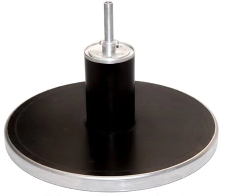
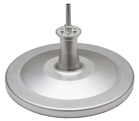
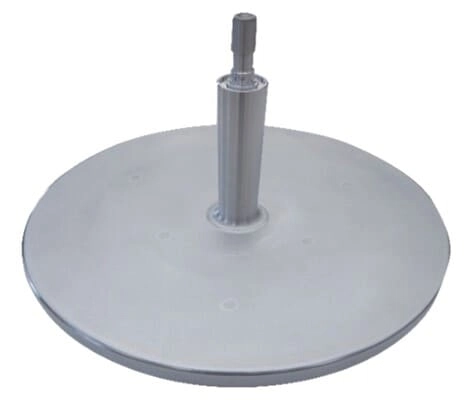
Accurately regulate chamber gas flow and vacuum levels, maintaining a stable deposition environment.Compatibility: Components are available in multiple sizes and specifications, designed to integrate with diverse CVD tool platforms.
Applications
- Semiconductor manufacturing: Deposition of dielectric layers, protective coatings, diffusion layers, and epitaxial wafers.
- Process optimization: Enhancing uniformity, yield, and reproducibility in CVD thin-film applications.