
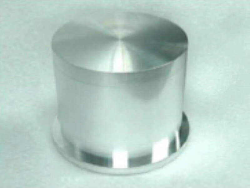


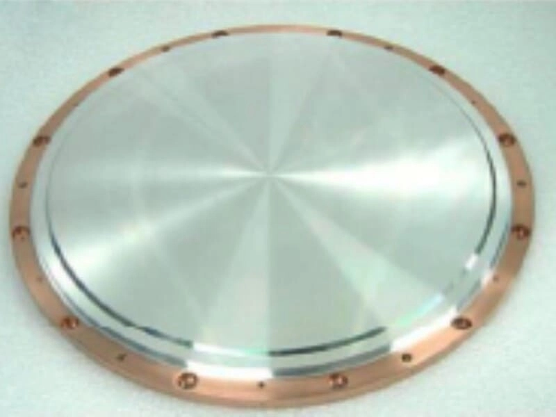
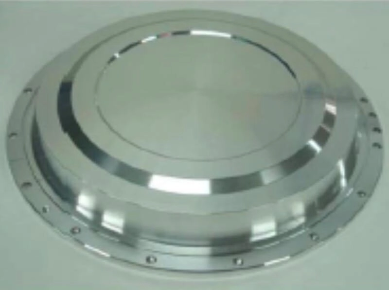



Model number: p-01
Sputtering Targets
High Purity × Diverse Materials × Precision Manufacturing
Scientia supplies high-purity sputtering targets that are widely used in the semiconductor, optoelectronics, and precision electronics industries. In advanced processes and thin-film deposition, the purity and stability of the target material play a decisive role in film performance and production yield. With strict process control, we deliver sputtering targets up to 5N (99.999%) purity, meeting the demanding requirements for material consistency and reliability in high-end semiconductor manufacturing.
Key Features & Advantages
High Purity Standards
-
Up to 5N (99.999%) purity for minimal particles and process stability.
-
Ensures superior thin-film quality in advanced applications.
Wide Material Coverage
-
Available in pure metals, alloys, and oxides (Al, Ti, Ta, Cu, W, Ni, Cr, NiV, ITO, ZnO).
-
Flexible options to match diverse process requirements.
Precision Processing & Testing
-
Advanced methods: vacuum melting, HIP, precision grinding, polishing.
-
Rigorous testing ensures high density and dimensional accuracy.
Material Categories
|
Al |
Ti |
Ta |
Cu |
W |
Ni |
Cr |
NiV |
ITO |
ZnO |
|
|---|---|---|---|---|---|---|---|---|---|---|
|
Pure Metals |
V |
V |
V |
V |
V |
V |
V |
|
|
|
|
Alloys |
|
|
|
|
|
|
|
V |
|
|
|
Metal Oxides |
|
|
|
|
|
|
|
|
V |
V |
Applications
-
Semiconductor Manufacturing: Thin-film deposition and barrier layers in PVD processes.
-
Optoelectronics: Display panels, optical coatings, and sensor production.
-
Precision Electronics: Hard disk read heads, MEMS devices, and high-frequency communication components.
-
Third-Generation Semiconductors: Metallization and packaging processes for SiC and GaN substrates.
Looking for reliable sputtering targets? Get in touch today for data sheets and solutions.